Rapid digitization across the globe has led to an unprecedented increase in the demand for semiconductor chips and displays. India being a very big consumer for end-products of semiconductor chips, semiconductor consumption in 2019 was a massive US $21 billion in 2021, most of which came from imports and this consumption is growing at the rate of 15 percent according to the data released by India Electronics and Semiconductor Association (IESA). India’s semiconductor consumption is expected to cross US $80 billion by 2026 and US $110 billion by 2030. [1] Despite this large semiconductor consumption, an Indian semiconductor fab (short for ‘fabrication plant’, and also called Foundry) with state-of-the-art technology had still remained a distant dream for India. The advanced technological ecosystem needed for semiconductor fabrication plants is mainly concentrated in countries like Taiwan, China, South Korea and Vietnam. The only established fab facility available in India even as of today is ‘Semiconductor Laboratory’ (SCL), Mohali. But, even today, SCL is capable of only a 180 nm technological process/node [2] (Note – technological process/node loosely correlates with the transistor size and consequently chip size. The most advanced technological process/node developed as of today is 3nm and 5nm) and doesn’t have state-of-the-art technology (like 45 nm) which could be used in high-end consumer electronics.
At the same time, the changing geopolitics leading to a hostile environment between China and the West (especially on issues like Taiwan and in the backdrop of Covid-19) nudged the companies who had a very strong base in China to spread out their operations by expanding outside of China as part of their ‘China plus one’ strategy. In addition to this, issues like global chip shortage and supply chain disruptions due to Russia-Ukraine war have nudged the big economies and semiconductor companies to re-strategize and operate in the chip-making business with a renewed push. India realised that as an emerging technological leader, it could be a very viable alternative for semiconductor companies planning to diversify their operations outside of China, which still continues to be a major hub for semiconductor fabrication.
Story So Far
In light of these facts, the Government of India recognised the need for and prospects of establishing semiconductor and display fabrication plants within the country and organised the Semicon India program on 15th December, 2021 with an outlay of INR 76,000 crore worth of PLI (Production Linked Incentives) schemes to attract investors and facilitate the development of semiconductors and display manufacturing ecosystem in India [3]. In addition, the MEITy also announced DLI (Design Linked Incentives) schemes and sought applications from hundred companies, MSMEs (Micro, Small and Medium Enterprises) and Start-ups to drive global and domestic investments for IP rights, design softwares, etc. The key objectives of Semicon India programme being – setting up semiconductor and display fabs, developing R&D & design capabilities in the Indian ecosystem and reducing import of semiconductors and displays by making India more self-sufficient.
As per the Modified Incentive Scheme for Semiconductor Chip-Making [4], the Ministry provides a fiscal support of 50% for all technological nodes of semiconductor fabrication and for specified technologies of Display manufacturing through these PLI schemes. This modified scheme also provides a special emphasis on 45nm semiconductor chips as they are economical, have high demand, less time-consuming, and have immense applications in automotive, telecom and power industries.
In response to these schemes and incentives, the Government of India received applications (as on February 19, 2022) from five major companies to establish chip and display manufacturing units in India with an investment of approximately $20.5 billion USD. The project proposals for semiconductor fabs [5] were –
Taiwanese chipmaker Foxconn and Indian multinational company Vedanta signed an MOU (Memorandum of Understanding) to set up in Gujarat a ₹1,54,000 crore semiconductor fabrication plant.
Singapore’s IGSS Ventures announced that it would be setting up a $3 billion plant in Tamil Nadu.
An International consortium named ISMC announced setting up of a $3 billion USD plant in Karnataka.
The two companies who submitted applications for Display Fabs were Vedanta and Elest. [3] The fiscal support sought from the government is about $ 2.7 billion USD out of the total projected investment of $ 6.7 billion USD
In addition, during Prime Minister Narendra Modi’s recent visit to USA, semiconductor companies Micron Technology and Applied Materials announced that they would set up new facilities for semiconductor chip manufacturing in India.[7] While Micron Technology confirmed that it would be investing on a new 2.75 billion USD assembly and test plant for semiconductor chips, Applied Materials confirmed a gross incremental investment of 400 million USD over four years for establishment of a Semiconductor Centre for Commercialization and Innovation in India.
As part of the Semicon India programme, SCL Mohali has been handed over from the Department of Space to the Ministry of Electronics and Information Technology (MEITy) of Government of India in an attempt to modernise and refurbish it into a commercial fab through joint ventures with other commercial fabs.
Except for the fabrication process, all the other processes and stages of chip design cycle happen in India and engineers in India have the skills required for all these other processes. The only missing links in semiconductor chip design cycle to ensure the complete cycle happens in India, are fabrication plants and the skills required among the Indian engineers to work in these fabs. Thus, the Government of India is very keen on promoting – 1) establishment of fabs 2) Developing required skill set among engineers here 3) Manufacturing of semiconductor chips and display units in India.
Thereby the Government intends to not only reduce the country’s semiconductor import, but also to provide employment opportunities in the related fields and make India a leading contender in the field of Semiconductor and Display manufacturing in the longer run.
Challenges
But despite the government’s best intent and immense efforts and the positive response received from the semiconductor companies on their keenness to invest in India and establish semiconductor industries, there are some very imminent key challenges, bottlenecks and roadblocks [6] which would come in the way of fruition of this mission –
1. Manufacturing of semiconductor chips and displays are very resource-hungry processes. The fabs need a) Large areas of land for setting up even a single fab and would need an even larger area to build a cluster of fabs close to each other to make it more cost-efficient. b) A very good supply of pure water as fabs are big hoggers of clean water. c) Uninterrupted power supply free of glitches as glitches can affect the very fine geometry of today’s semiconductor chips. c) A very diligent maintenance of an extremely hygienic environment to prevent entry of impurities into the chip.

In a country like India where the resources are limited and the marginalised are still deprived of these very same resources, the decision to set up such resource-hungry industries must be taken after careful analysis of whether it is worth the trade-off and also considering ways in which we can make up at least to some extent for the enormous amount of resources consumed by these industries.
2. In addition to the resources, fabs also need some rare earth metals in their fabrication process. As India has very limited supply of these elements, they have to necessarily be imported from other countries like China. Thus, on one hand, we have the prospects and benefits of – (a) Achieving long-term goals of self-sufficiency in semiconductor chips & display manufacturing (b) Being a key player in semiconductor industry (c) Transfer of technology and skillset (d) Employment generation.
And on the other side, we have the cons of import costs of materials like rare earth metals and enormous resource consumption by fabs. A thorough cost-benefit is very much a necessity in gauging if the benefits outweigh the costs or if it would be more viable to continue importing Semiconductor chips and Displays as before.
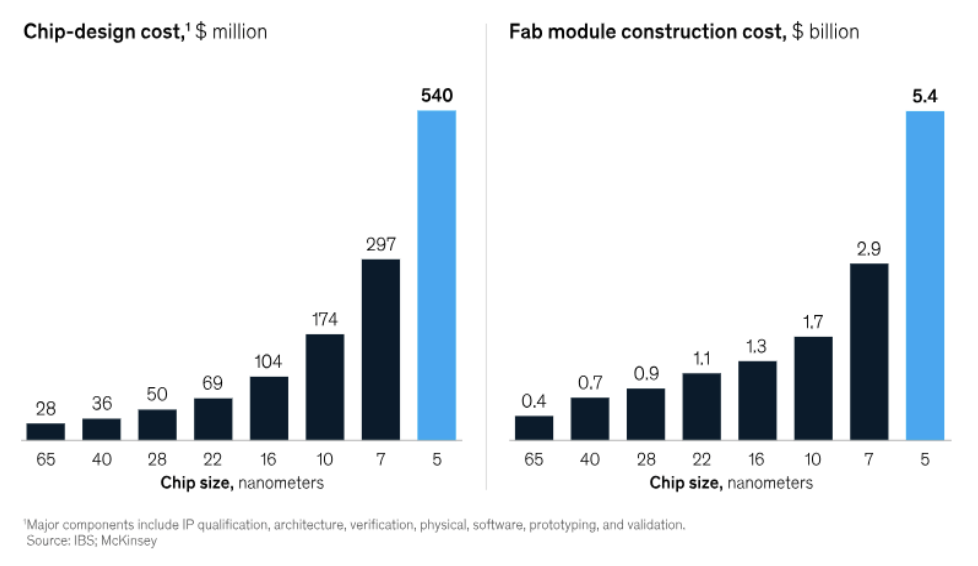
3. India is starting in the semiconductor race quite late compared to countries which are already established semiconductor hubs, like China, South Korea, Taiwan, etc. With advances in semiconductor physics, the fabs established in these countries would continue to come up with even smaller nodes and newer technologies, which would have much higher complex & costlier chip-design cycles and fab construction processes than that of the larger nodes (Refer Fig. 2). And they would also need dedicated R&D and more sophisticated infrastructure facilities for fabrication. Thus, the fabrication plant for a certain older/larger node even if set up in India, we have a long way to go in catching up with the ever-evolving industry in terms of technology standards, expertise and efficiency and becoming a prominent trusted manufacturer in the global market. As to how long it might take for India to get in par with the industry, it remains to be seen.

4. The delay in catching up with the industry has other consequences too. Till the Indian fabs achieve a reasonable level of expertise and efficiency in fabrication, the orders which the Indian fabs receive could be lower compared to the full capacity of the fab. As fabs operate 24*7, there should be a large number of chip orders (including both domestic consumption and export) for the fab to ensure the full utilisation of the fab. If the fab is not run at a minimum of 90 percent of full capacity almost round the clock, chip fabrication gets very costly due to poor utilisation of fab capacity. Due to this, the costly semiconductor chips fabricated in India would not appeal to the consumers and they would become uncompetitive in the global market compared to the big players who have been in the semiconductor industry for a long time.
5. Lack of skilled workforce of trained semiconductor engineers trained in process technology and device physics, which are very much required in operations of fabrication plants. A very rigorous upskilling programme is to be undertaken in order to solve this problem of lack of skilled workforce
In the face of such imminent challenges and bottlenecks, India’s long-term semiconductor dream of being ‘Aatma Nirbhar’ (self-sufficient) and even being an exporter in the global market for semiconductor chips and displays remains a very ambitious one, but maybe one worth pursuing!
References
- https://www.business-standard.com/article/current-affairs/india-s-own-semiconductor-consumption-to-cross-80-bn-by-2026-pm-modi-122050500990_1.html
- https://www.scl.gov.in/cmos_fab_facility.html
- https://pib.gov.in/PressReleasePage.aspx?PRID=1799621
- https://pib.gov.in/PressReleaseIframePage.aspx?PRID=1928479
- https://www.drishtiias.com/daily-updates/daily-news-analysis/modified-incentive-scheme-for-semiconductor-chip-making
- https://www.businesstoday.in/technology/top-story/story/india-must-overcome-key-challenges-to-become-semiconductor-superpower-says-father-of-pentium-vinod-dham-358578-2023-01-02
- https://www.businesstoday.in/technology/news/story/micron-applied-materials-lam-research-announcements-could-generate-80000-high-skills-jobs-in-india-mos-it-386873-2023-06-23

